Wooden Desk Lamp

Wooden Desk Lamp

DIY Wooden Desk Lamp

First of all make triangle base of dimension 150mm x 90mm x 19mm board.

Then take two wooden pieces of dimension 430mm x 50mm and 300mm x 50mm.

Take smaller piece (300mm x 50mm) and cut the end at 70 degree both side but opposite to each other.

Now take larger piece (430mm x 50mm) and make grove into it for led placement.

Take smaller piece (300mm x 50mm) and make a grove behind it and insert pipe for wiring to pass through and then seal it with wood filling.

Place led strip in to grove and cover it with acrylic sheet, pass wire through the pipe (inserted in samller wood) and then to the base.

Attach the top wood to the smaller wooden piece and together attach them to wooden base piece.
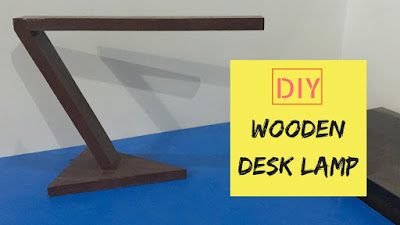
Fill all the voids with woodfilling and then sand it with fine sand paper for better result. Then apply some paint on it and you are ready to go...

Finshed Product...
Wooden Desk Lamp

Watch & Subscribe

Popular posts from this blog

7447 Seven Segment Display Working

The 7447 chip is used to drive 7 segment display.  You must use the 7447 with a common anode 7-segment display.  The input to the 7447 is a binary number DCBA where D is 8s, C is 4s, B is 2s and A is 1s. The inputs DCBA often come from a binary counter. Output Pin Diagram This pin diagram of 7447 IC where  Pin 7 - A Pin 1 - B Pin 2 - C Pin 6 - D In Seven Segment Display (Common Cathode) Pins are represented by alphabets on display as well as on 7447 ic For more details have look at circuit diagram below Circuit Diagram  This is whole working circuit for seven segment display R0 - 390 ohms (Led with dip switch resistance ) R1 - 100 ohms R2 - 1k ohms

Nifty 50

HDFC HDFC HDFC HDFC 3 Column Layout Column 1 Content for the first column. Column 2 Content for the second column. Column 3 Content for the third column.

Shift Registers with circuit diagram

    The 74xx595 devices contain an 8-bit, serial-in parallel-out (SIPO). The storage register has parallel 3-state outputs. Separate clocks are provided for both the shift and storage register. The shift register has a direct overriding clear (SRCLR) input, serial (SER) input and serial outputs for cascading. When the output-enable (OE) input is high, the output are in high impedance state. Pin Configuration Circuit Diagram This Switch Diagram Configuration is for Data, Out-Enable, Latch, Clock Pins as shown above in picture This is whole working circuit for shift register but there is a slight change in the Clear Pin, in this push button is grounded Vcc - 5Volts R1 - 1k ohms C - 47microfard R2 - 1k ohms R3 - 10k ohms QH' - This is for the next shift register to make 16 bit ouput led and so on. (This pin 9 goes to the DATA PIN of next shift register) Watch video for more details...