7447 Seven Segment Display Working


7447 ic pin


The 7447 chip is used to drive 7 segment display. 
You must use the 7447 with a common anode 7-segment display. The input to the 7447 is a binary number DCBA where D is 8s, C is 4s, B is 2s and A is 1s. The inputs DCBA often come from a binary counter.

Output


Pin Diagram

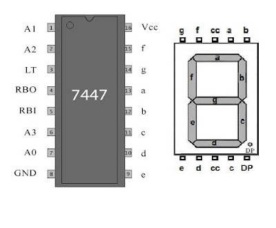
Pin Diagram of 7447
This pin diagram of 7447 IC where 
Pin 7 - A
Pin 1 - B
Pin 2 - C
Pin 6 - D

In Seven Segment Display (Common Cathode)
Pins are represented by alphabets on display as well as on 7447 ic
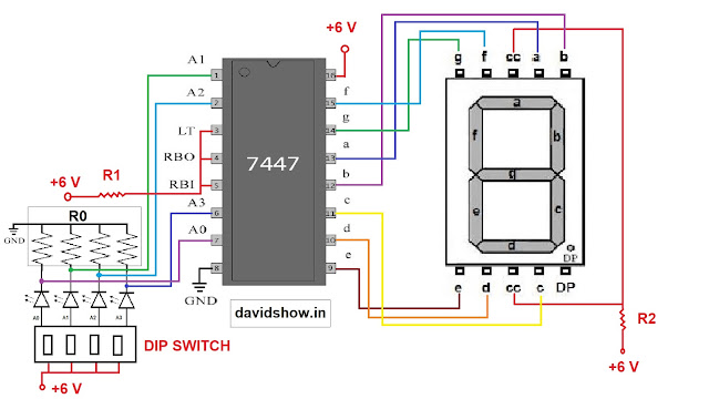
For more details have look at circuit diagram below

Circuit Diagram 

Circuit Diagram of 7447

This is whole working circuit for seven segment display

R0 - 390 ohms (Led with dip switch resistance )
R1 - 100 ohms
R2 - 1k ohms

Watch the video for more details...


Popular posts from this blog

Nifty 50

HDFC HDFC HDFC HDFC 3 Column Layout Column 1 Content for the first column. Column 2 Content for the second column. Column 3 Content for the third column.

Shift Registers with circuit diagram

    The 74xx595 devices contain an 8-bit, serial-in parallel-out (SIPO). The storage register has parallel 3-state outputs. Separate clocks are provided for both the shift and storage register. The shift register has a direct overriding clear (SRCLR) input, serial (SER) input and serial outputs for cascading. When the output-enable (OE) input is high, the output are in high impedance state. Pin Configuration Circuit Diagram This Switch Diagram Configuration is for Data, Out-Enable, Latch, Clock Pins as shown above in picture This is whole working circuit for shift register but there is a slight change in the Clear Pin, in this push button is grounded Vcc - 5Volts R1 - 1k ohms C - 47microfard R2 - 1k ohms R3 - 10k ohms QH' - This is for the next shift register to make 16 bit ouput led and so on. (This pin 9 goes to the DATA PIN of next shift register) Watch video for more details...